APPLICATION
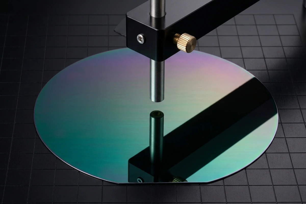
SiO₂ Thickness Measurement
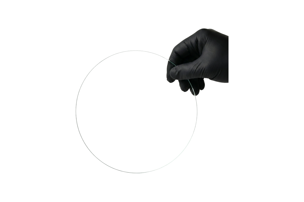
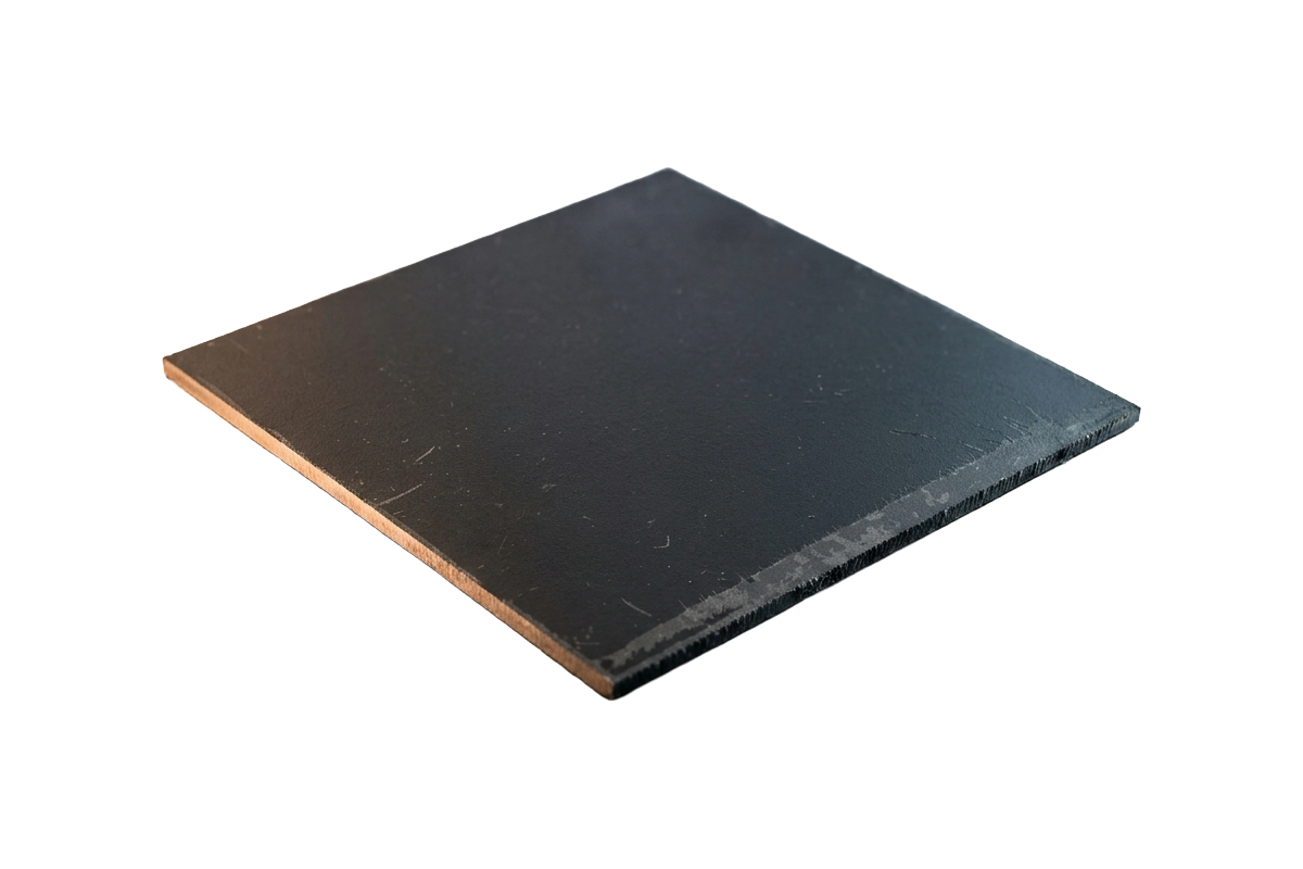
Oxide thickness measurement for semiconductor, display, MEMS, and optical device applications.
SiO₂Si waferTFM-100
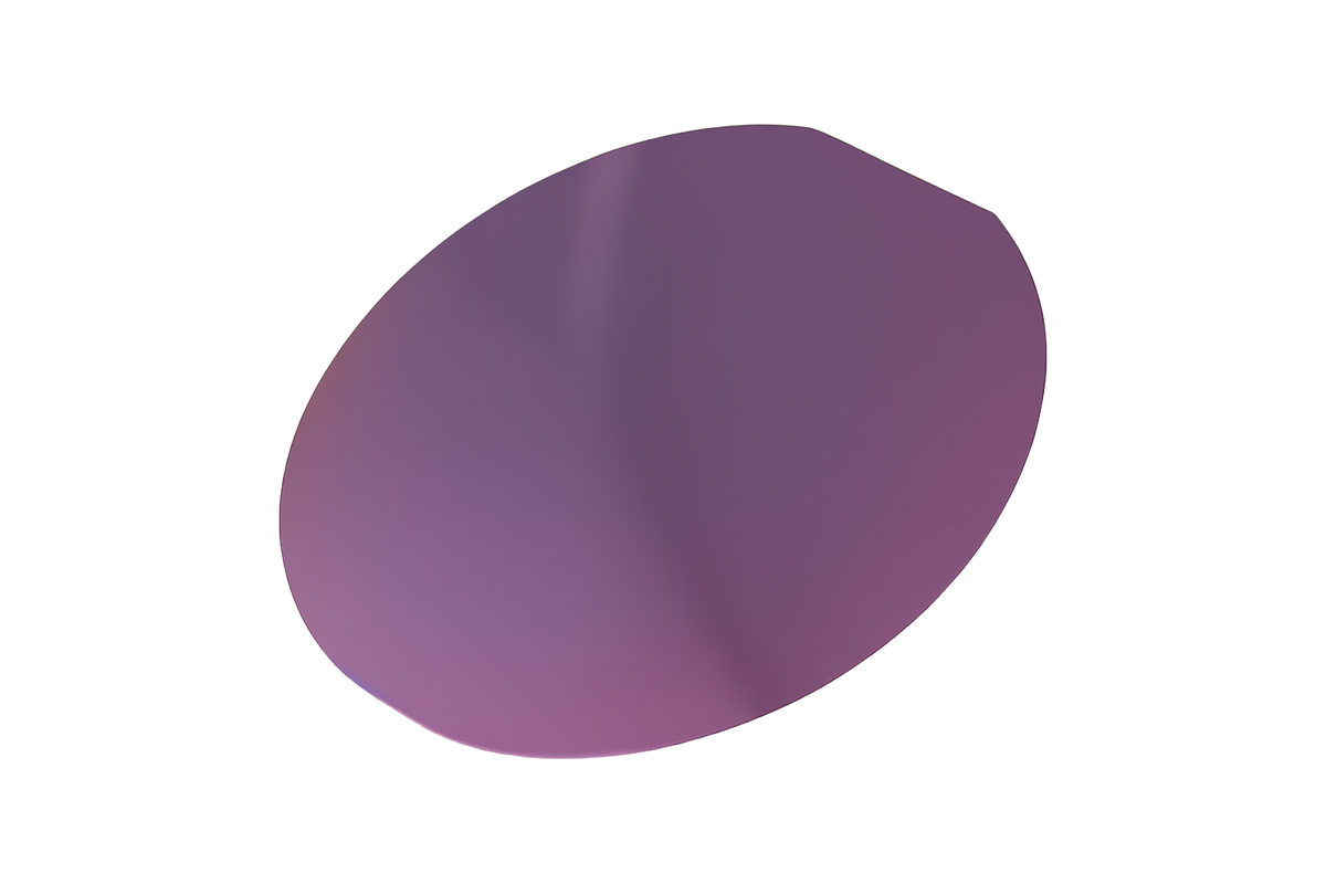
Oxide thickness measurement for semiconductor, display, MEMS, and optical device applications.
Model selection depends on the film stack, substrate, target thickness range, surface condition, and optical contrast.
Explore nearby applications without going back to the applications list.
TFM system selection depends on sample geometry, required throughput, and measurement workflow.