TFM-500
XY motorized thickness mapping system
A motorized TFM system for automated multi-point thickness mapping on wafer, glass, panel, and process samples.
XY mappingPractical workflowRaw data review
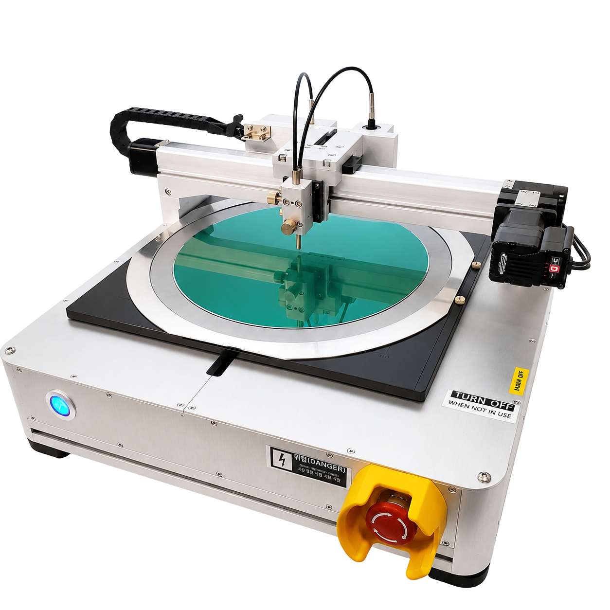
A motorized TFM system for automated multi-point thickness mapping on wafer, glass, panel, and process samples.
Core strengths for this TFM system.
Defines measurement points and runs automated spectra acquisition across the selected area.
Supports a 300 × 300 mm rectangular measurement area for wafers, glass, panels, and large samples.
Stores spectra, coordinates, recipe, and results for later point review and re-analysis.
Define points, measure, map, and review results in one continuous workflow.
Model options and common specifications.
| Model | Wavelength Range | Thickness Range* | Same-point Repeatability Reference |
|---|---|---|---|
| TFM-500 Standard | 350–1050 nm | 15 nm – 100 µm* | 500 nm SiO₂ reference sample, n=10 |
| TFM-500 NIR | 750–1100 nm | 1 µm – 500 µm* | 850 / 1000 nm SiO₂ reference sample, n=10 |
| TFM-500 XT | 1005–1080 nm | 100 µm – 2,000 µm* | 2000 nm SiO₂ or transparent reference film, n=10 |
* Depending on sample condition, film stack, substrate, optical contrast, and measurement recipe.
| Measurement method | Reflectance-based thin-film thickness mapping |
|---|---|
| Motion system | Motorized XY stage |
| Standard sample support | Up to 12-inch wafers and 300 mm × 300 mm square samples. |
| Wafer loading guide | Supports round wafers and square panel-type samples. |
| Optional stage | 370 mm × 470 mm motorized stage option. |
| Software | Lite included |
| Data review | Mapping point spectra, coordinates, recipe, and results can be stored for later review and re-analysis |
| Z-axis support options | Z-map height compensation and camera-assisted autofocus options depend on sample flatness, spot size, and workflow |
| Light source | Tungsten-halogen standard; UV-VIS broadband source optional |
| Recommended installation space | Approx. 1000 mm × 800 mm laboratory table |
| Power input | Single-phase AC 100–240 V, 50/60 Hz (220 V standard) |
| Recommended available power | 500 W |
| Standard sample | The reference sample is 500 nm SiO₂. Nominal 850 nm, 1000 nm, and 2000 nm options are available on request. |
Standard support includes wafers up to 12 inches and square samples up to 300 mm × 300 mm. Sample handling also depends on the fixture and measurement access.
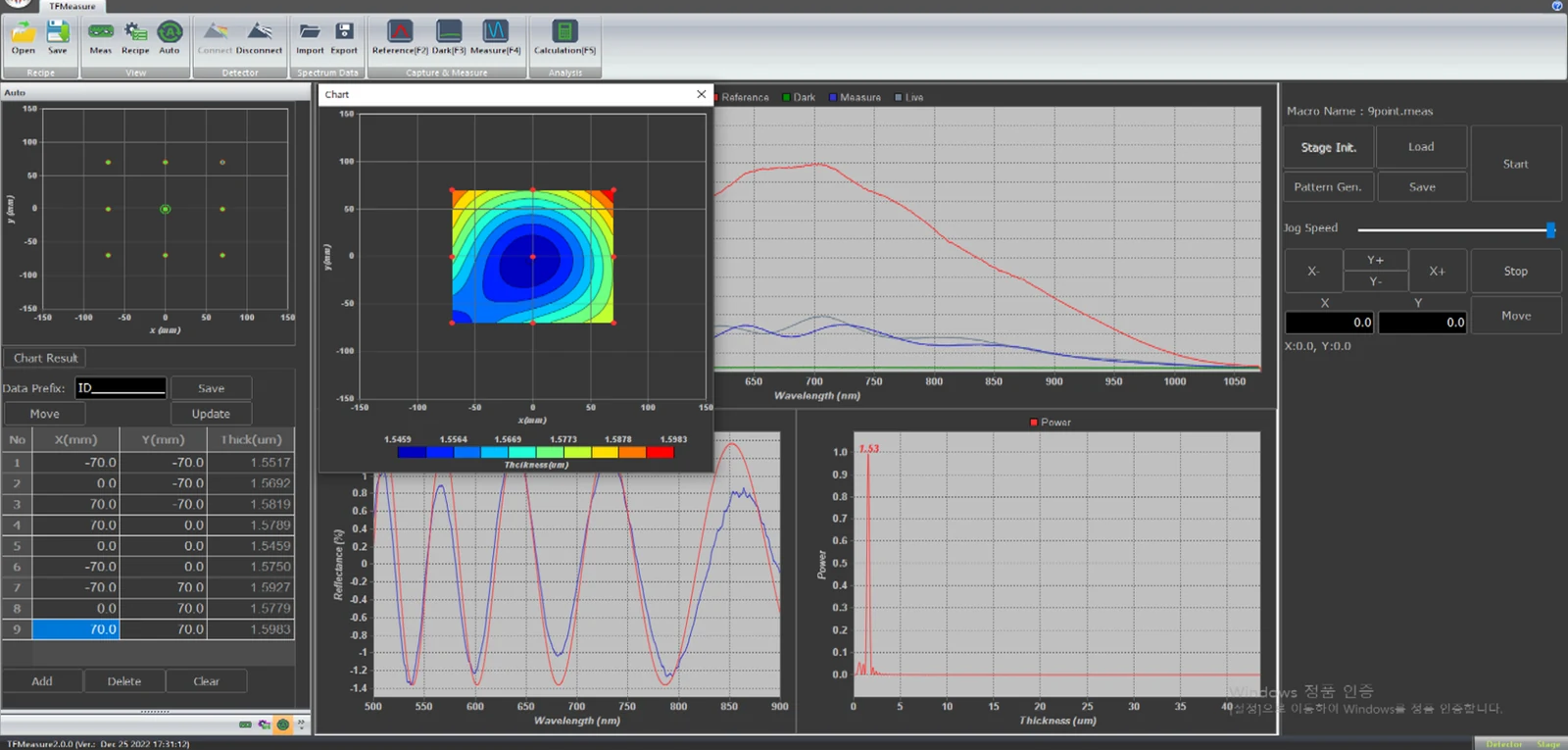
The mapping workflow helps define measurement coordinates, run automated spectra acquisition, and review thickness results as both a map and a table.
Each mapping point can be stored with its raw spectrum, coordinate, recipe, and result for later review and re-analysis.
Users can review selected point spectra and re-apply adjusted analysis settings across saved mapping data without repeating the full acquisition.
Typical samples and coating structures for this TFM system.
Common accessories for this TFM measurement setup.